For nearly a century, digital technology has operated under a strict binary regime. The entire modern world, from tiny microcontrollers in household appliances to massive data centers driving global communications, relies on the simple choice between zero and one. This binary foundational layer was not chosen because it represents the peak of mathematical efficiency. When Claude Shannon formalized the connection between electronic switching circuits and Boolean algebra in the late 1930s, he established a practical framework that prioritized engineering simplicity over structural optimization. Early electrical engineers found it incredibly easy to build switches that were either completely on or completely off. A voltage was either clearly present or completely absent, creating a robust, noise-tolerant environment that allowed the semiconductor industry to scale exponentially for decades.
However, as engineers push traditional silicon to its absolute physical limits, alternative foundational designs are returning to the spotlight. At the forefront of this architectural re-evaluation is ternary computing architecture, a system that replaces the traditional binary bit with a three-state digit known as a trit. Instead of restricting data processing to two absolute values, a ternary system introduces a third state, unlocking an entirely different paradigm for data density, computational speed, and energy efficiency.
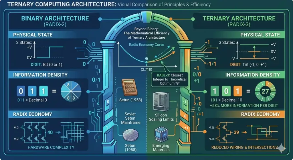
To understand the core appeal of a ternary computing architecture, one must look at a mathematical concept known as the radix economy. The radix economy evaluates the structural cost of representing numbers within a specific base system. Mathematically, the total hardware cost of storing a range of numbers up to a certain value is determined by multiplying the radix, or base, by the number of digits required to express that value. When mathematicians map this efficiency curve across all possible base systems using continuous calculus, they discover that the absolute most efficient base for a computing machine is Euler’s number, a mathematical constant roughly equal to $e \approx 2.718$.
Because it is impossible to build physical hardware based on a fractional radix, engineers must select the closest whole number integer. Three is mathematically closer to Euler’s number than two. This means that a base-3 system is theoretically the most hardware-efficient way to process numbers, requiring roughly 5.4% fewer total logical components than a binary system to manage the exact same range of information. By fundamentally reducing the volume of internal wiring, logic gate intersections, and buses required on a microchip, this structural edge offers a direct pathway to lower latency and reduced energy consumption.
From Wooden Calculators to Soviet Mainframes
The concept of a ternary computing architecture is far from a modern novelty. Its roots extend deep into the history of mechanical and electrical engineering, predating the silicon transistor by more than a century. The earliest functional realization of base-3 computation arrived in 1840, when an English inventor named Thomas Fowler constructed a mechanical calculating machine built entirely from wood and iron rods. Fowler was tasked with calculating complex local property taxes, a process that involved non-decimal currency systems. He discovered that utilizing balanced ternary logic, which uses the states of minus one, zero, and plus one, allowed his mechanical machine to perform complex multi-digit calculations with a fraction of the physical parts required by standard decimal or binary mechanical counters. Fowler’s machine layout proved that three-state systems could drastically simplify physical execution mechanics.
The true golden age of physical ternary hardware arrived during the mid-twentieth century inside the laboratory of Moscow State University. In 1958, a team of Soviet engineers led by Nikolai Brusentsov developed the Setun, the world’s first fully operational electronic ternary computer. While Western institutions focused entirely on perfecting binary mainframes, Brusentsov’s team recognized that the scarcity of reliable electronic components in the post-war Soviet Union demanded a more efficient architecture.
The Setun operated on a balanced ternary system using magnetic core memory and vacuum tubes. Because the architecture was inherently more elegant than its binary counterparts, the Setun required significantly fewer components to perform equivalent mathematical tasks. The magnetic cores used in the machine naturally possessed three stable magnetic states, making them an ideal fit for the logic paradigm without requiring complex voltage regulation tricks. The computer possessed an innate resistance to arithmetic errors and proved remarkably resilient in real-world operations, rarely suffering from the hardware failures that plagued early Western binary mainframes. A total of fifty Setun computers were manufactured and deployed across various Soviet universities and research centers, where they handled complex scientific modeling and industrial calculations for over a decade.
Despite the technical triumphs of the Setun and its subsequent upgrade, the Setun-70, the broader geopolitical and industrial tides turned decisively against the three-state model. The global semiconductor pipeline focused its massive financial and manufacturing resources entirely on standardizing binary silicon logic gates. As mass production scaled, the cost of binary transistors plummeted, rendering the structural efficiency gains of ternary hardware economically irrelevant for a time. The Soviet administrative state eventually ceased funding for the Setun project in favor of cloning Western binary IBM architectures, forcing base-3 hardware into the margins of computer science history for the remainder of the twentieth century.
The Sinking Shield of Silicon Scaling
The resurgence of interest in ternary computing architecture during the current era is driven by raw physical necessity rather than academic curiosity. For over fifty years, the technology sector thrived on the predictable rhythms of Moore’s Law, which dictated that the number of transistors packed onto a microchip would double roughly every two years. This relentless miniaturization allowed binary processors to become faster and more power-efficient purely through physical scaling, as shrinking components required less voltage and switched states more rapidly.
That scaling paradigm has hit a brick wall. Modern transistor gates are now so microscopically small that they are approaching the width of individual atoms, measuring just a few nanometers across. At this scale, quantum mechanics introduces a destructive phenomenon known as electron leakage or quantum tunneling. Electrons begin to spontaneously jump through physical insulated barriers even when a transistor is switched completely off, causing binary chips to waste massive amounts of electricity as pure heat. This thermal barrier has created the phenomenon of dark silicon, where significant portions of a modern processor must remain powered down or throttled during operation to prevent the physical chip from melting itself.
At the same time, the global explosion of data processing demands, particularly within heavy mathematical workloads like modern artificial intelligence, deep learning, and advanced simulation software, has exposed the fundamental bottlenecks of binary data buses. A binary chip must move immense oceans of ones and zeros across physical wires to perform basic matrix multiplications and comparative operations. This massive movement of data between the processor and memory creates a severe hardware bottleneck, consuming immense amounts of power and generating massive data center electric bills.
This landscape makes a ternary computing architecture incredibly attractive to contemporary hardware engineers. By moving away from the binary constraint, a three-state architecture allows designers to fundamentally increase the information density of a processor without needing to shrink physical transistors any further. Instead of forcing a chip to struggle against the laws of atomic physics, a ternary approach shifts the innovation vector from raw physical scaling to logical architecture optimization, offering an elegant escape hatch from the limitations of traditional binary silicon.
Modern Explorers Mapping the Ternary Frontier
Rather than remaining confined to theoretical research papers, modern ternary computing architecture projects are actively materializing across corporate research laboratories, academic centers, and open-source hardware communities. These modern initiatives are successfully bridging the historic gap between abstract multi-valued logic and physical hardware implementation, proving that base-3 infrastructure can be realized using contemporary design tools.
A significant corporate development in this field emerged from a patent disclosure filed by the global telecommunications giant Huawei. The design details an innovative ternary logic gate circuit specifically optimized for deployment inside high-performance electronic chips and computing devices. Huawei’s architecture utilizes a three-state logic system representing values of minus one, zero, and positive one across a specialized three-transistor configuration. By handling multi-valued addition and subtraction natively at the hardware level, this design aims to drastically reduce the total number of transistors required on a processor surface, targeting a substantial drop in energy consumption for power-hungry processing clusters.
Simultaneously, industrial and academic collaborations in South Korea have achieved major milestones in physical fabrication. A research team at the Ulsan National Institute of Science and Technology, backed by long-term research funding from Samsung, successfully demonstrated the world’s first unbalanced ternary semiconductor design manufactured directly onto a large-scale commercial wafer. Instead of relying on negative voltages, this specific architecture utilizes states of zero, one, and two, strategically using the third state to actively contain and suppress leakage current. The breakthrough demonstrated that multi-valued computing structures can be successfully manufactured using existing commercial foundry lines, clearing a major economic hurdle for future production.
On the architectural design front, the Ternary Research Group at the University of South-Eastern Norway has been systematically building an open-source technology stack to support base-3 hardware. Founded by academic researchers, the group is actively developing specialized Electronic Design Automation tooling capable of designing and verifying mixed-radix computing systems. Their ongoing projects include the creation of functional compilers that can translate standard programming languages directly into native ternary assembly code.
Furthermore, the open-source hardware community has demonstrated that functional ternary hardware is viable through projects like the 5500FP processor. Developed as a 24-trit device implemented on modern Field Programmable Gate Array hardware, this project acts as a functional, open-source ternary Reduced Instruction Set Computer platform. It allows engineers and independent developers to write, debug, and execute native ternary programs, creating a hands-on workbench that demystifies multi-valued computing for a new generation of engineers.
Mathematical Magic and Native Negative Numbers
The operational superiority of a ternary computing architecture is rooted in the distinct ways a three-state system organizes and processes information at the foundational level. While a binary bit holds a single piece of information based on two states, a single ternary trit possesses an informational value calculated as $\log_2(3) \approx 1.585$ bits of data. This means that a ternary system delivers a 58% leap in information density per digit over binary. A data bus built on a ternary architecture can transmit significantly larger numeric values using fewer physical wires and fewer processor cycles, instantly streamlining internal chip communications.
The mathematical advantages multiply when looking at balanced ternary logic, which defines its three states as negative one, zero, and positive one. In a standard binary processor, representing a negative number requires a complex engineering workaround known as two’s complement. This system forces the chip to dedicate its most significant bit purely to tracking whether a number is positive or negative, requiring extra logic gates and additional clock cycles to perform basic sign-flipping operations during arithmetic tasks.
Balanced ternary completely eliminates this overhead. Because negative values are built directly into the foundational logic layer, negative numbers are represented naturally without any structural penalties. To change the sign of any balanced ternary value, a circuit simply has to invert the states of the individual trits, turning positive ones into negative ones and vice versa. As a result, subtraction operations inside the processor are executed exactly like standard addition operations, radically simplifying the arithmetic logic unit and bypassing the traditional computational tax associated with negative values.
Beyond basic arithmetic, a ternary computing architecture dramatically accelerates data comparison operations. When a traditional binary chip needs to determine if a value is greater than, equal to, or less than another value, it must execute multiple sequential checks, testing conditions step-by-step through a series of logical gates. A ternary logic gate can resolve this exact comparison in a single operation cycle, outputting one of its three distinct states to immediately signal the result. This native three-way branching capability provides massive algorithmic speedups for database sorting, search routing, and complex matrix processing operations.
Bridging the Binary Divide via Mixed Radix Systems
Despite the clear mathematical and efficiency benefits of a pure ternary computing architecture, it cannot simply replace the existing technological ecosystem overnight. The global technology infrastructure represents trillions of dollars in entrenched binary investments, spanning manufacturing foundries, software operating systems, and billions of lines of legacy application code. To find a viable path toward commercial adoption, ternary technology must adapt to this existing gravity through a hybrid paradigm known as mixed-radix computing.
A mixed-radix system integrates ternary components directly into a broader binary environment, allowing both architectures to do what they do best. Instead of demanding a complete rewrite of global software infrastructure, a mixed-radix approach deploys specialized ternary co-processors and accelerators alongside standard binary central processing units. The binary CPU manages standard operating system tasks and traditional application layers, while passing intensive mathematical matrix workloads directly to the ternary accelerator.
This evolutionary transition is already quietly occurring at the interface level of mainstream consumer hardware. As physical data transmission wires hit bandwidth limits, high-speed connection standards like USB 4.2, Thunderbolt 5, and next-generation GDDR7 graphics memory have started deploying multi-level signaling protocols such as Pulse Amplitude Modulation 3. Rather than transmitting standard binary pulses, these interfaces use three distinct voltage levels across the physical copper lines to carry data.
By treating the physical transmission wire as a temporary ternary data bus, these standards can move significantly more data per clock cycle without requiring higher operating frequencies or generating destructive amounts of thermal noise. This successful deployment proves that the tech industry is entirely willing to embrace three-state logic when the physical limitations of binary systems threaten to stall commercial progress.
Beyond Silicon Transistors to Quantum Horizons
The long-term roadmap for ternary computing architecture extends far beyond traditional silicon wafers. While projects like the Samsung-backed UNIST wafer prove that base-3 logic can run on standard metal-oxide semiconductors, the true performance potential of ternary systems will likely unlock through emerging materials science and non-silicon hardware horizons.
One of the most promising avenues involves carbon nanotube field-effect transistors. Carbon nanotubes possess extraordinary electrical properties that allow engineers to precisely tune their voltage thresholds. This material flexibility makes it significantly easier to build stable three-state logic gates without the heavy transistor count penalties that occur when forcing traditional silicon to handle a middle voltage state. Academic labs worldwide are heavily focusing on these carbon structures, filing a surging volume of research papers detailing nanotube-based ternary logic blocks.
Another revolutionary frontier is spintronic logic-in-memory architecture. Traditional computers waste massive amounts of time and energy shuffling data back and forth between a separate processor and a memory storage unit. Spintronics utilizes the inherent magnetic spin of electrons to store and process data simultaneously within the exact same physical location. Because electron spin states can naturally be oriented in multiple directions, spintronic hardware provides a perfect physical foundation for building low-power ternary chips that completely eliminate the traditional data transport bottleneck.
Finally, this architectural expansion is reshaping the cutting edge of quantum computing. While standard quantum computers utilize two-state quantum bits known as qubits, an emerging class of quantum hardware utilizes three-state quantum variables called qutrits. By leveraging the principles of quantum superposition across three distinct energy levels simultaneously, a qutrit-based quantum system gains an exponential expansion in computational state space compared to a qubit system. This non-binary quantum advancement demonstrates that whether looking at mechanical rods, corporate silicon patents, or the atomic realm of quantum mechanics, the path toward the future of computing is increasingly clearing a way for the power of three.
References
- Fowler’s Ternary Calculating Machine History
- Ternary RISC Processor Achieves Non-Binary Computing Via FPGA
- University of South-Eastern Norway Ternary Research Group Stack
- Huawei Ternary Logic Gate Circuit Patent Details
- UNIST and Samsung Wafer Semiconductor Development
- Ternary Logic vs Binary Logic Comparative Analysis Video